How do you guarantee 100% material integrity and full traceability for every batch?
To guarantee the reliability required for semiconductor applications, our facility implements a rigorous approach to material integrity and traceability. We manage every batch through a closed-loop system defined by the following controls:
- Stringent source validation: We only procure raw materials from audited and approved mills. Every delivery must be accompanied by an original mill test report, which we verify against the specific chemical and physical requirements of the semiconductor industry before any processing begins.
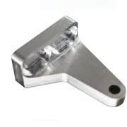
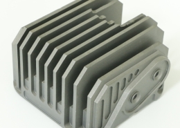
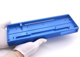
- Unique batch serialization: Upon arrival, each material lot is assigned a unique internal tracking number. This ID follows the material through every stage of production—from initial cutting and semiconductor cnc machining to final surface treatment—ensuring an unbroken link between the raw stock and the finished component.
- Material verification and inspection: We perform incoming inspections to confirm that raw materials match required specifications. Material certificates are cross-referenced with internal records to ensure consistency and prevent material mix-ups before production begins.
- Comprehensive documentation: For every shipment, we provide a full data package, including material certifications and certificates of compliance. This level of transparency ensures that every component is fully traceable back to its source, meeting the audit requirements of semiconductor equipment manufacturers.
Is your surface finish truly functional, or just visually acceptable?
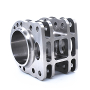
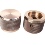
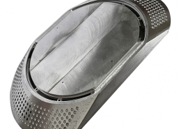
In the context of Semiconductor cnc machining, surface finish is prioritized for its functional role in vacuum performance and contamination control. We recognize that visual uniformity does not guarantee technical compliance. Our processes are designed to achieve specific Ra and Rz values that assist in managing particle entrapment and maintaining surface integrity. For high-vacuum components, we implement controlled machining strategies and specialized secondary processes like electropolishing when required to minimize surface irregularities. These finishes are monitored to ensure they meet the specific technical requirements of sensitive semiconductor environments. Verification is performed using surface profilometers to confirm that the functional topography aligns with engineering specifications, ensuring the component supports operational stability and cleanliness requirements without relying on cosmetic appearance alone.